For sake of simplicity, we first consider the wave propagation of a
collimated incident beam into a planar waveguide. This particular structure
is formed of three step-index infinite planar layers (see Fig.
3). Light can be observed at the structure output
provided that total reflection occurs at each interface and constructive
interferences occur between two successive reflected wavefronts (A and C in
the figure). The first condition implies that a high-index layer is
sandwiched between two low-index layers and gives the range of acceptable
incident angle. The second condition translates into a phase difference
between the wavefronts A and C multiple of 2![]() . Therefore the range
of acceptable incident angles is no longer continuous but discrete. A
single-mode waveguide is a guide which can propagate only the direction
parallel to the waveguide. The core layer thickness ranges between
. Therefore the range
of acceptable incident angles is no longer continuous but discrete. A
single-mode waveguide is a guide which can propagate only the direction
parallel to the waveguide. The core layer thickness ranges between
![]() and
and ![]() depending on the index difference. Multimode
guide propagates beams coming from different directions.
depending on the index difference. Multimode
guide propagates beams coming from different directions.
In practice, one needs the full electromagnetic field theory to compute the beam propagation inside the waveguide. The continuity relations of the electromagnetic fields at each interface lead to the equations of propagation of guided modes [Jeunhomme (1990)]. Depending on the wavelength and the guide thickness (l in the Fig. 3), these equations have either no solution (structure under the cutoff frequency), either only one solution (single-mode structure) or several ones (multi-mode structure). The number of solutions also depends on the difference of refractive index between the various layers of the structure. The larger the index difference are, the better the modes are confined. These equations also allow to estimate the energy distribution profile which can be approximated, to first order, by a Gaussian function. The major part of the energy lies in the channel, but evanescent waves can interact with evanescent waves coming from other close waveguides (see the directional coupler in Sect. 3.3).
In interferometry, multi-mode guided structures cannot be used since there exist optical path differences between the various modes. In the following, only single-mode waveguides are considered.
A first method to build integrated guides on planar substrate is based on
glass ion exchange [Ramaswamy & Srivastava (1988),Ross (1989)]: the ![]() ions of a glass
substrate are exchanged by diffusion process with ions (
ions of a glass
substrate are exchanged by diffusion process with ions (![]() ,
,![]() or
or ![]() ) of molten salts. The local modification of
the glass chemical composition increases the refractive index at the glass
surface. A three-layer structure (air/ions/glass) is created and the
light is vertically confined. By standard photo-masking techniques (see
Fig. 4), the ion exchange can be limited to a compact
area and create a channel waveguide. Since ion exchange only occurs at the
surface of the glass, the last step of the process consists in embedding
the guide, either by forcing the ions to migrate with an electric field or
by depositing a silica layer on the waveguide. We obtain a component which
guides the light like an optical fiber, the ion exchange area being the
core and the glass substrate
) of molten salts. The local modification of
the glass chemical composition increases the refractive index at the glass
surface. A three-layer structure (air/ions/glass) is created and the
light is vertically confined. By standard photo-masking techniques (see
Fig. 4), the ion exchange can be limited to a compact
area and create a channel waveguide. Since ion exchange only occurs at the
surface of the glass, the last step of the process consists in embedding
the guide, either by forcing the ions to migrate with an electric field or
by depositing a silica layer on the waveguide. We obtain a component which
guides the light like an optical fiber, the ion exchange area being the
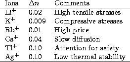
core and the glass substrate![]() being the cladding. According to the ions of the molten salt, the
refractive index difference can vary between 0.009 and 0.1 (see
Table 1). This technology provides various components for
telecom and metrology applications.
being the cladding. According to the ions of the molten salt, the
refractive index difference can vary between 0.009 and 0.1 (see
Table 1). This technology provides various components for
telecom and metrology applications.
Another method consists of etching layers of silicon of various indices
[Mottier (1996)]. These layers can be either phosphorus-doped silica or
silicon-nitride. Both technologies can create channels by etching
layers of material, where light is confined like in an optical fiber (see
Fig. 5). The channel geometry is defined by
standard photo-masking techniques. According to the fabrication process,
![]() can be either high (0.5) for very small sensors, or very low
(between 0.003 and 0.015) for a high coupling efficiency with optical
fibers. These technologies usually provide components for various
industrial applications (gyroscopes, Fabry-Pérot cavities or
interferometric displacement sensors).
can be either high (0.5) for very small sensors, or very low
(between 0.003 and 0.015) for a high coupling efficiency with optical
fibers. These technologies usually provide components for various
industrial applications (gyroscopes, Fabry-Pérot cavities or
interferometric displacement sensors).
Single mode waveguides made by direct UV light inscription onto polymers are in progress. Such a technology is still in development and the components present usually high propagation losses [Strohhöfer et al. (1998)].
The first two technologies provide many standard
functions for wavelengths ranging between 0.5 ![]() and 1.5
and 1.5 ![]() (standard telecom bands). Several examples are presented (see
Fig. 6):
(standard telecom bands). Several examples are presented (see
Fig. 6):
Copyright The European Southern Observatory (ESO)
![\begin{figure}
\begin{center}
\leavevmode
\includegraphics [angle=-90,width=0.6\columnwidth]{functions.ps}
\end{center}\end{figure}](/articles/aas/full/1999/13/ds1695/img26.gif)