A number of workers have investigated devices which contain trapping
layers, to enhance the multiple tunneling, for application at X-ray
wavelengths (Gaidis et al. 1996;
Mears et al. 1993; Poelaert et al. 1996). The results described here are for a tantalum based STJ whose
geometry is illustrated in Fig. 1 (click here). The device consists of a ![]() m square
100 nm thick epitaxial tantalum film on a smooth sapphire substrate on top
of which a 30 nm thick aluminium trapping layer is deposited. The
insulating barrier, of order 1 nm thick, is formed through a controlled
oxidation of this aluminium. The oxide barrier is capped by a further 30 nm
aluminium trapping layer followed by a thin seed layer prior to the
deposition of 100 nm of polycrystalline tantalum. The leads are 2
m square
100 nm thick epitaxial tantalum film on a smooth sapphire substrate on top
of which a 30 nm thick aluminium trapping layer is deposited. The
insulating barrier, of order 1 nm thick, is formed through a controlled
oxidation of this aluminium. The oxide barrier is capped by a further 30 nm
aluminium trapping layer followed by a thin seed layer prior to the
deposition of 100 nm of polycrystalline tantalum. The leads are 2 ![]() m wide
and made of niobium to prevent quasiparticle losses down the leads from the
lower bandgap materials of tantalum and aluminium. Further details on these
devices can be found in Verhoeve et al. (1996a), while the role of the
aluminium trapping layers is discussed in Poelaert et al. (1996). The
original theoretical concept of quasiparticle trapping is described by
Booth (1987).
m wide
and made of niobium to prevent quasiparticle losses down the leads from the
lower bandgap materials of tantalum and aluminium. Further details on these
devices can be found in Verhoeve et al. (1996a), while the role of the
aluminium trapping layers is discussed in Poelaert et al. (1996). The
original theoretical concept of quasiparticle trapping is described by
Booth (1987).
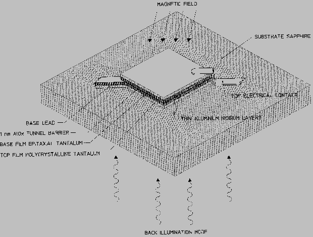
Figure 1: A schematic of the tantalum tunnel junction used in the current experiments
together with it's orientation in a parallel magnetic field so as to
suppress the Josephson current. The device is operated in a back illuminated
mode therefore the UV response is limited by the cut-off of the substrate
Prior to establishing the optical performance of the device the key
electrical characteristics were derived through the investigation of the
I-V function at 0.3 K. The bandgap of the device at the barrier was
determined to be ![]() meV. This is lower than that for bulk
tantalum
meV. This is lower than that for bulk
tantalum ![]() meV due to the proximity effect induced by the
aluminium trapping layers. The resistivity of the barrier was estimated to
be
meV due to the proximity effect induced by the
aluminium trapping layers. The resistivity of the barrier was estimated to
be ![]() while the leakage current was
while the leakage current was ![]() at
at ![]() mV.
mV.
The optical experiments have been performed in a ![]() cryostat at a base
temperature of
cryostat at a base
temperature of ![]() K. As shown in Fig. 1 (click here), the device was illuminated
through the sapphire substrate (back illuminated), via a fibre optic, by
photons from a monochromatic xenon lamp light source. The illumination was
initially at a very low intensity level
K. As shown in Fig. 1 (click here), the device was illuminated
through the sapphire substrate (back illuminated), via a fibre optic, by
photons from a monochromatic xenon lamp light source. The illumination was
initially at a very low intensity level ![]() ) such that only a single
optical photon was incident on the detector during the tunnel and
electronics processing time. All optical illumination described here was in
this back-illuminated mode. This mode is preferred for two reasons: i) all
optical photons are absorbed in the high quality epitaxial tantalum film,
the charge from which is trapped by the aluminium film close to the
barrier. Note the top polycrystalline film will have a coating of tantalum
oxides
) such that only a single
optical photon was incident on the detector during the tunnel and
electronics processing time. All optical illumination described here was in
this back-illuminated mode. This mode is preferred for two reasons: i) all
optical photons are absorbed in the high quality epitaxial tantalum film,
the charge from which is trapped by the aluminium film close to the
barrier. Note the top polycrystalline film will have a coating of tantalum
oxides ![]() nm thick (Peacock et al. 1997a) which may absorb a significant
fraction of the optical photons if illumination was from the front. The
resultant charge from photons absorbed in this oxide layer may well become
trapped by such oxides. ii) The back illumination mode means that optical
photons are not blocked by the lead to the top film. While this latter
problem is minor for a single device, it would become a major issue when
operating arrays where the number and layout of the top film connecting
leads would cover a significant part of the top surface of the array.
nm thick (Peacock et al. 1997a) which may absorb a significant
fraction of the optical photons if illumination was from the front. The
resultant charge from photons absorbed in this oxide layer may well become
trapped by such oxides. ii) The back illumination mode means that optical
photons are not blocked by the lead to the top film. While this latter
problem is minor for a single device, it would become a major issue when
operating arrays where the number and layout of the top film connecting
leads would cover a significant part of the top surface of the array.
The electrical signals from the STJ were read out using a charge sensitive
amplifier operated at room temperature about 1 m from the device. Each
detected optical photon gives rise to a pulse at the output of the
preamplifier. The amplitude of this pulse is measured together with the
pulse rise time and corresponds to the total number of tunnelled electrons
(charge output) and signal decay time respectively. The electronic noise
is continuously monitored through the response to an electronic pulse fed
directly into the pre-amplifier. Typical noise values of
![]() electrons
electrons ![]() nm at
nm at ![]() nm) were obtained. Here
nm) were obtained. Here
![]() represents the
full width at half maximum (FWHM) of the typically gaussian shaped charge
distribution. Further details of the experimental configuration can be
found in Peacock et al. (1996, 1997a) and
Verhoeve et al. (1997).
represents the
full width at half maximum (FWHM) of the typically gaussian shaped charge
distribution. Further details of the experimental configuration can be
found in Peacock et al. (1996, 1997a) and
Verhoeve et al. (1997).