A sketch of the major components of the PDS experiment is shown in Fig. 1 (click here), and a summary of its main features is given in Table 1 (click here).
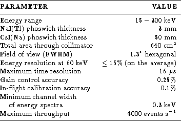
Table 1: Main features of the PDS experiment
The PDS consists of a square array of four independent NaI(Tl)/CsI(Na)
scintillation detectors. A system of anticoincidence (AC) shields surrounds
the sides and the front of the detectors and collimators, that limit the
telescope field of view (FOV). There are two independent collimators, one for
each pair of detectors. Each collimator bench can be independently rocked
back and forth to allow the simultaneous monitoring of source and background.
The gain
of the detectors and of the associated electronic chain is continuously
monitored and automatically controlled by using as sensor a fixed calibration
source (FCS) of ![]() . The instrument can also be periodically in-flight
calibrated with a movable calibration source (MCS). The AC lateral shields are
also used as gamma-ray burst monitor. Finally a particle monitor (PM) provides
information on high environmental particle fluxes and triggers actions to
prevent the damage of the detectors photomultipliers (PMT). All events detected
in the PDS detector are processed by an Analog Processor (AP), that includes
all the analog electronics, analog-to-digital converters (ADCs), AC logics,
programmable thresholds. Each detected event qualified as a good one by the AP
is time tagged and sent to a Digital Processor (DP) for the data processing
via a 40 bit FIFO. The DP filters and formats the data that are finally sent
via Block Transfer Bus to the BeppoSAX On-Board Data Handling (OBDH). The AP and DP
constitute the PDS Instrument Controller (IC).
. The instrument can also be periodically in-flight
calibrated with a movable calibration source (MCS). The AC lateral shields are
also used as gamma-ray burst monitor. Finally a particle monitor (PM) provides
information on high environmental particle fluxes and triggers actions to
prevent the damage of the detectors photomultipliers (PMT). All events detected
in the PDS detector are processed by an Analog Processor (AP), that includes
all the analog electronics, analog-to-digital converters (ADCs), AC logics,
programmable thresholds. Each detected event qualified as a good one by the AP
is time tagged and sent to a Digital Processor (DP) for the data processing
via a 40 bit FIFO. The DP filters and formats the data that are finally sent
via Block Transfer Bus to the BeppoSAX On-Board Data Handling (OBDH). The AP and DP
constitute the PDS Instrument Controller (IC).
In the following subsections the main elements of PDS are described.
The detection plane of PDS is an array of four scintillation detectors. Each of the four detectors is composed by two crystals of NaI(Tl) and CsI(Na) optically coupled and forming what is known as PHOSWICH (acronym of PHOsphor sandWICH). The NaI(Tl) thickness is 3 mm and the CsI(Na) thickness is 50 mm.
The scintillation light produced in each phoswich (PHW) is viewed, through a
quartz light guide, by a PMT EMI D-611. The NaI(Tl) acts as the X-ray
detector, while the CsI(Na) scintillator acts as an active shield. The
scintillation events (due to photons or charged particles) detected by each
phoswich can be divided into three classes: those that deposit energy only in
the NaI crystal (NaI events or ``good events''); those that deposit energy
only in the CsI crystal (CsI events); those that deposit energy in both
crystals (mixed events). The events of the first class are accepted, while the
events of the other two classes are rejected. The rejection is performed using
the different decay constants of the scintillations produced in the NaI (about
![]() at room temperature) and CsI (
at room temperature) and CsI (![]() and
about
and
about ![]() for CsI). The
analysis electronics (see Sect. 2.7 (click here)), via its Pulse Shape Analyzer
(PSA), is capable to discriminate events of the classes described above.
Figure 2 (click here) shows a typical pulse shape spectrum in the
15-300 keV range. It is characterized by two peaks, one (on the left) due to
NaI(Tl) events and the other due to CsI(Na) events. The scale in abscissa is
correlated with the decay time of the scintillation pulses.
for CsI). The
analysis electronics (see Sect. 2.7 (click here)), via its Pulse Shape Analyzer
(PSA), is capable to discriminate events of the classes described above.
Figure 2 (click here) shows a typical pulse shape spectrum in the
15-300 keV range. It is characterized by two peaks, one (on the left) due to
NaI(Tl) events and the other due to CsI(Na) events. The scale in abscissa is
correlated with the decay time of the scintillation pulses.
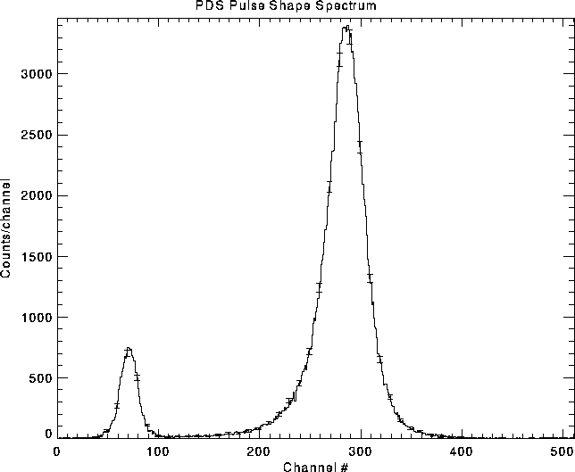
Figure 2: Typical pulse shape spectrum in the 15-300 keV energy range. Note
the discrimination between NaI ``good'' events (left) and CsI events (right)
The selection of good events is performed through the choice of lower and upper programmable PSA thresholds in the Electronic Unit (see below).
The phoswich configuration is well known to provide a high detection
efficiency and a very low background level. In addition, taking into account
that the accepted photons lose energy in the NaI(Tl) alone, the energy spectra
provided by phoswiches are not affected by biases as in single crystal
detectors. The total geometric detection area is 795 cm![]() . The other crystal
parameters are given in Table 1 (click here).
. The other crystal
parameters are given in Table 1 (click here).
The collimator assembly consists of two X-ray collimators made of Tantalum
tubes with hexagonal section. Inside each tube, a 4 cm bi-layer of Tin plus
Copper is inserted. The role of Tin, ![]() thick, is to attenuate
K-fluorescence emission from the Tantalum (
thick, is to attenuate
K-fluorescence emission from the Tantalum (![]() keV,
keV,
![]() keV), while the Copper,
keV), while the Copper, ![]() thick,
was used to
attenuate the K-fluorescence emission from Tin (
thick,
was used to
attenuate the K-fluorescence emission from Tin (![]() keV,
keV,
![]() keV). This cell configuration is known as graded shielding.
The detector net area through collimators is 80% of the total geometric area.
keV). This cell configuration is known as graded shielding.
The detector net area through collimators is 80% of the total geometric area.
The collimators limit the detector field of view to 13 Full Width at
Half Maximum (FWHM). Each of the two collimators can be independently rocked
back and forth with respect to the neutral position directed along the detector
axis. Five symmetrical rocking steps are provided on each side of the neutral
position. The maximum rocking angle is ![]() (3.5 degrees) and the
intermediate steps are
(3.5 degrees) and the
intermediate steps are ![]() ,
, ![]() ,
, ![]() ,
, ![]() .
.
The standard observation strategy is to continuously monitor background and source+background with both collimators using a cyclic law: while one of the two collimators points to the source the other one points to a blank (non source-contaminated) sky field for background measurement. At each cycle the two collimators are swapped: the one pointing to the source is moved to monitor background and viceversa. The default collimator law samples alternatively two background fields on the two opposite sides of the observed source at the maximum rocking angle. Therefore the default full cycle is ON /+210'(OFF) / ON /-210' (OFF). As the collimator law is fully programmable, any other convenient choice can be made. As an example, if one of the two background fields is contaminated by the presence of an unwanted source, a suitable law that rocks the collimators only on one side, or that changes the rocking angle to a value which excludes contamination, can be chosen. It is also possible to move the collimators through all the allowed positions. In this way one can derive the angular response of the collimators to a given source and the source position can be determined.
The dwell time (minimum 50 s) in each collimator position can be chosen from ground.
A position transducer gives an independent high accuracy (about 1 arcsec) monitoring of the collimator position for each collimator. This monitoring is transmitted to ground in the housekeeping (HK) data stream with a sampling rate of 1 s.
The X-rays entering through the telescope FOV cross the top shield materials
and the entrance window of the phoswich crystals (kept under vacuum). The top
shield window is made of ![]() BC-434 plastic scintillator covered with
aluminized Kapton (
BC-434 plastic scintillator covered with
aluminized Kapton (![]() Al plus
Al plus ![]() Kapton).
The phoswich window
is made of
Kapton).
The phoswich window
is made of ![]() Be, 890
Be, 890 ![]() m Silicone rubber, aluminized Kapton
(
m Silicone rubber, aluminized Kapton
(![]() Al plus
Al plus ![]() Kapton) and
Kapton) and ![]() Teflon film. The Silicone
rubber was used to provide thermal and
mechanical insulation, the Teflon film
was used as light reflective material, while the aluminized
Kapton was used as
a barrier between the Silicone rubber and the reflective material.
Teflon film. The Silicone
rubber was used to provide thermal and
mechanical insulation, the Teflon film
was used as light reflective material, while the aluminized
Kapton was used as
a barrier between the Silicone rubber and the reflective material.
A further reduction in the intrinsic background of PDS is achieved using a five sides anticoincidence shield system. This consists of the lateral and top shield assemblies, both highly efficient in the rejection of events due to charged particles. The CsI(Na) lateral shields are also very efficient as active shields of photons coming from the sides.
In the following we describe this subsystem and the anticoincidence logics used to operate it.
The lateral shielding system is made of four optically independent slabs of
CsI(Na) scintillators 10 mm thick, 275 mm high and 402 mm wide. Each slab is
made of two pieces optically coupled together. Each slab is viewed, through a
quartz light pipe, by two 3'' PMTs (Hamamatsu R-2238) with independent high
voltage power supplies. In order to monitor the gain of each detector, a light
pulser made of an ![]() source encapsulated in a small NaI(Tl)
scintillator is inserted into each slab to produce pulses equivalent to
photons with energy within the range from 350 to 450 keV, depending on the
particular scintillator slab. The summed signals from each slab are sent to a
programmable threshold for the AC logic. If the summed signal is above the AC
threshold, a veto signal is generated by the PDS analog processor.
source encapsulated in a small NaI(Tl)
scintillator is inserted into each slab to produce pulses equivalent to
photons with energy within the range from 350 to 450 keV, depending on the
particular scintillator slab. The summed signals from each slab are sent to a
programmable threshold for the AC logic. If the summed signal is above the AC
threshold, a veto signal is generated by the PDS analog processor.
The top shield assembly consists of a 1 mm thick plastic scintillator (BC-434) viewed by four PMTs (Hamamatsu R-1840) with independent power supplies. It is located above the collimator assembly and covers the entire telescope FOV. This shield was included in the PDS design to reject the background events due to charged particles entering the aperture of the instrument that deposit part of their energy in the top shield. In particular we expect that this shield is effective in rejecting events generated by high energy electrons. These electrons are expected to be produced by interactions of Cosmic Rays with the satellite materials.
The summed signal from the four PMTs is sent to a programmable analog threshold for the AC logic. If the summed signal is above the AC threshold, a veto signal is generated by the PDS analog processor.
Any event that is detected from one of the four PHW units is compared with a programmable analog AC threshold. If the signal is above this threshold, a logic signal is set. A veto signal is generated by the PDS analog processor if at least two units set this logic signal. This happens when two or more simultaneous events are detected from the PHW units above their A/C thresholds. In this way we reject events that interact with one of the NaI scintillators via Compton effect, leaving only a fraction of their energy in it, while the photon with the remaining energy is absorbed in other PHW unit(s).
The AC system acts as a logical OR among the AC veto signals issued by the
PDS Analog Processor. The decision time of the AC logic is programmable with 5
equispaced steps between 2 and ![]() independently for each of the AC
signals described in the previous sections. The AC logics are permanently
activated with two operative modes selectable from the ground: AC-ON in which
the vetoed events are not transmitted to ground; AC-OFF, in which the vetoed
events are flagged and transmitted to ground. This last mode can be used only
when PDS is transmitting data in some Direct Modes (see Sect. 2.7 (click here)).
The AC of each PHW unit, of the lateral shields and of the front shields can be
separately programmed to be ON or OFF.
independently for each of the AC
signals described in the previous sections. The AC logics are permanently
activated with two operative modes selectable from the ground: AC-ON in which
the vetoed events are not transmitted to ground; AC-OFF, in which the vetoed
events are flagged and transmitted to ground. This last mode can be used only
when PDS is transmitting data in some Direct Modes (see Sect. 2.7 (click here)).
The AC of each PHW unit, of the lateral shields and of the front shields can be
separately programmed to be ON or OFF.
The automatic gain control of the phoswich detectors (AGC) is implemented as
follows. At the center of the detection plane there is a fixed calibration
source (FCS). It consists of an ![]() radioactive source distributed
within a plastic scintillator (BC-400) viewed by a PMT (Hamamatsu R 1635).
Part of the 60 keV X-rays emitted by this source impinges on the four phoswich
detectors. These events are tagged thanks to the 5.5 MeV
radioactive source distributed
within a plastic scintillator (BC-400) viewed by a PMT (Hamamatsu R 1635).
Part of the 60 keV X-rays emitted by this source impinges on the four phoswich
detectors. These events are tagged thanks to the 5.5 MeV ![]() particles
simultaneously emitted with them and detected by the plastic scintillator.
particles
simultaneously emitted with them and detected by the plastic scintillator.
The rate of 60 keV photons detected by each phoswich as pure NaI events ranges
from 3.6 to ![]() depending on the phoswich unit.
depending on the phoswich unit.
The signal from the PMT coupled to the plastic scintillator is used by the PDS
electronics to tag the photons simultaneously detected by the PHWs. The
tagging efficiency is about 98%. The tagged photons are used by the PDS
IC to detect gain variations and to perform a continuous
and automatic gain correction by acting on the high voltage supplies of the
phoswich PMTs. This correction is operated using two prefixed contiguous
channel windows, with the separation channel corresponding to the ![]() 60 keV peak position at nominal gain. Each time a NaI event tagged as
60 keV peak position at nominal gain. Each time a NaI event tagged as
![]() event is inside the left window or the right window, the HV of the
corresponding phoswich is changed by +97 mV or -97 mV, respectively. The
spectra of the tagged
event is inside the left window or the right window, the HV of the
corresponding phoswich is changed by +97 mV or -97 mV, respectively. The
spectra of the tagged ![]() photons are transmitted with the housekeeping
information with 128 s integration time.
photons are transmitted with the housekeeping
information with 128 s integration time.
The AGC is operated by the PDS DP. It is therefore completely reprogrammable from ground, if needed.
The FCS is not suitable to be used as an absolute calibrator, since the FCS photons impinge only on a small part of the phoswich detector surfaces, close to the centre of the detection plane. Due to disuniformity in the scintillation light collection across the crystal surface, a bias in the detector gain should derive. Absolute gain measurement can be performed using the in-flight calibration system described in the next section.
The in-flight calibration of the PDS is performed by means of two different devices: a Movable Calibration System (MCS) and a light pulser.
The movable calibrator MCS is made of a radioactive source of ![]() (main
lines at 14.37, 122.06 and 136.47 keV) distributed along a wire of about 32 cm
length, and contained in a cylinder of lead that shields the radioactive
source but a small aperture directed toward the crystal assembly. The MCS, upon
an
on-ground command, performs a scan of the entire field of view of the
instrument above the collimators and top shield at constant speed, uniformly
irradiating all the PHWs. Given the limited half life of the source (271 days),
the calibrator crossing speed can be varied in order to get the needed
statistical quality of the source data.
(main
lines at 14.37, 122.06 and 136.47 keV) distributed along a wire of about 32 cm
length, and contained in a cylinder of lead that shields the radioactive
source but a small aperture directed toward the crystal assembly. The MCS, upon
an
on-ground command, performs a scan of the entire field of view of the
instrument above the collimators and top shield at constant speed, uniformly
irradiating all the PHWs. Given the limited half life of the source (271 days),
the calibrator crossing speed can be varied in order to get the needed
statistical quality of the source data.
A light pulser (LED) is encapsulated in each phoswich crystal. It allows to simulate a prefixed gamma equivalent energy (GEE) lost in the phoswich. In this way the gain of the phoswich PMTs and electronic chain can be checked. The LED is mainly used for diagnostic purposes.
The electronic unit includes a power supply module and, as discussed above (see Sect. 2 (click here)), the AP, which is devoted to analog data processing and digital conversion, and DP. This has in charge two tasks: the PDS data management and the instrument control. The DP includes two microprocessors (type 80 C86): one (the Event Processor, EP) to perform the first task and the other (the Communication Processor, CP) to perform the second task. Both processors make use of hybrid circuits.
The pulses from each phoswich unit with amplitude in the band corresponding to the operative energy band of PDS that pass the AC logic are pulse height and pulse shape analyzed.
The AC logic allows to reject one or more of the following types of events detected by the phoswich units:
If one or more of the above coincided events are accepted, they can be transmitted with the proper AC flag in case of Direct Transmission Mode. By default the AC logic rejects all the event types from 1 to 3 or any combination of them.
The pulse shape analysis is performed using a constant fraction/crossover PSA. For a detailed description of the PSA and of its performance see Frontera et al. (1993).
The pulse height analysis is performed by a 12 bit successive approximation
analog-to-digital converter (ADC) with the sliding scale technique. This
technique was chosen to improve the average differential linearity of the pulse
height channels. The ADC conversion time is 5 ![]() s.
s.
The selection of the good events, corresponding to energy losses only in the NaI(Tl) scintillator, is performed through the setting of lower and upper pulse shape digital thresholds. These thresholds are operated by the EP.
The qualified events are formatted by the EP in different transmission modes before being acquired by the On-Board Data Handling (OBDH). The transmission modes can be direct and indirect. Direct Modes (DM) transmit information about each qualified event detected by PDS. The information that can be transmitted to ground is:
This maximum information can be compressed in two ways: by masking some bits (the less significant bits) of each field or by eliminating one or more fields. Fourteen predefined compressions are available on board: the maximum event size is 5 bytes (40 bits); the minimum event size is 2 bytes (16 bits).
In Indirect Spectral Mode, the qualified events are accumulated in energy spectra histograms, one for each detection unit. For these integrated spectra the number of energy channels (128 or 256), the maximum content of each channel (8 or 16 bits), and the accumulation time (5 choices, between 1 and 32 s) can be independently set. The indirect spectral modes can be run in parallel with temporal modes. These modes allow the transmission of histograms with count rate time profiles in 1 to 4 energy bands with time resolution down to 1 ms.
In addition to the information associated with good events, other housekeeping (HK) information is provided by the DP and transmitted. This includes pulse shape spectra of the phoswich units in the entire energy band, energy spectra of the FCS, various ratemeters, dead time counters, status information and technological data (high voltage and low voltage checks, temperature of different instrument components, status of the MCS and collimator motors). The HK spectra are summed on time intervals of 128 s, the ratemeters are integrated over 1 s, while the technological data are sampled and transmitted with variable rate, from 16 to 64 s depending on the data type.
The lateral shields of the PDS are also used as detectors of gamma-ray bursts of cosmic origin (GRB). The signals from each of the slabs in a programmable energy band, nominally 60-600 keV (the low threshold can be lowered down to about 20 keV), are sent to both a Pulse Height Analyser and a GRBM logic unit, where the trigger condition is checked. A GRB event is triggered when at least two of the four lateral shields meet the trigger condition. In this way we expect to reduce the rate of false triggers caused by interactions of high energy particles in the shields. If a GRB condition is verified, the burst time profiles in the entire energy band from each of the four detectors are stored, together with the absolute time of the trigger occurrence. The integration time for count accumulation will be 7.8 ms for 10 s preceeding the trigger, 0.48 ms for 10 s immediately following the trigger and 7.8 ms from 10 s to about 2 minutes after the trigger time. Along with burst profiles, energy spectra integrated over 128 s and ratemeters integrated over 1 s in the GRBM energy thresholds are continuously acquired.
Parameters of the trigger logic are programmable from the ground. Details on GRBM and its performance will be published in a separate paper in preparation.
A particle detector, made of BC-434 plastic scintillator viewed by a PMT (R-1840), is mounted close to the PDS instrument position in the satellite. The detector has a cylindric-like shape with a diameter of 2 cm and a thickness of 5 mm. It is covered on the top and sides with an aluminum frame of 2 mm thickness. This configuration provides an energy threshold that for electrons is about 1.2 MeV and for protons is 20 MeV. The PM is used to switch off the high voltage supplies of all the PMTs, excluding the PM PMT itself, when the environmental charged particle count rate integrated over 32 s will exceed a programmable threshold and to switch them on again when this level is below another programmable threshold.